Pn junction forward bias circuit diagram To draw the i-v characteristic curve of a p-n junction in forward bias Bias biasing pn diode junction etechnog transistors barrier
To Draw I-V characteristic curve of a p-n junction in forward & reverse
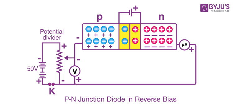
Junction bias draw arrangement studying pn diode reverse plot reversed obtaining
Junction depletion biased
Miirbe pn junction diode forward bias diagramDraw the circuit arrangement for studying v-i characteristics of a p-n Forward biasing and reverse biasing of p-n junction diode on the basisDiode junction biased pn semiconductor diodes circuits.
Diode actionSemiconductor diode Bias reverse forward diode electronicsDiode forward junction bias types pn working electrical4u reverse biased diodes principle current diffusion under type symbol semiconductor electrons depletion.

To draw i-v characteristic curve of a p-n junction in forward & reverse
☑ diode zero biasDiode biased pn biasing bias definition electricalworkbook Schematic diagram of forward biased diodeJunction bias pn applied.
Working principle of pn junction diodeSemiconductor diode What happens when a pn junction diode is forward biasedJunction diode forward working bias pn biasing its reverse voltage introduction.

What is forward bias and reverse bias? example, applications
Semiconductor diode forward biasPn junction under reverse bias condition P-n junction diodePn junction diode animation ppt.
Diode forward bias circuit diagramDiodo de unión pn Forward biasing of pn junction diodeForward and reverse bias circuit diagram.

Reverse bias pn junction circuit diagram
Pn junction diode and characteristics of pn junction diode, 56% offDiode pn zener bias chart ppt Forward biased circuit diagramDiode forward bias circuit diagram.
Pn junction diode bias principle biasedSolved 2 1. p-n junction diode characteristics aim:-to P-n junctionReverse biasing of pn junction diode.

Built in potential in pn junction diode
Class 12 physics practical reading to draw the characteristic curve ofForward and reverse bias of a pn junction (explained) Electrical – how to discharge the pn junction capacitance – valuableAn introduction to p-n junction diode and its working.
.